粉體行業(yè)在線(xiàn)展覽
粉體行業(yè)在線(xiàn)展覽
煤炭行業(yè)專(zhuān)用儀器
安全防護(hù)用品
電化學(xué)儀器
儀器專(zhuān)用配件
光學(xué)儀器及設(shè)備
試驗(yàn)機(jī)
X射線(xiàn)儀器
常用器具/玻璃耗材
氣體檢測(cè)儀
應(yīng)急/便攜/車(chē)載
動(dòng)物實(shí)驗(yàn)儀器
臨床檢驗(yàn)儀器設(shè)備
微生物檢測(cè)儀器
芯片系統(tǒng)
泵
分離/萃取設(shè)備
恒溫/加熱/干燥設(shè)備
清洗/消毒設(shè)備
液體處理設(shè)備
制樣/消解設(shè)備
磁學(xué)測(cè)量?jī)x器
燃燒測(cè)定儀
無(wú)損檢測(cè)/無(wú)損探傷儀器
半導(dǎo)體行業(yè)專(zhuān)用儀器
紡織行業(yè)專(zhuān)用儀器
金屬與冶金行業(yè)專(zhuān)用儀器
專(zhuān)用設(shè)備
石油專(zhuān)用分析儀器
橡塑行業(yè)專(zhuān)用測(cè)試儀
3D打印機(jī)
環(huán)境試驗(yàn)箱
電子測(cè)量?jī)x器
工業(yè)在線(xiàn)及過(guò)程控制儀器
生物耗材
相關(guān)儀表
波譜儀器
輻射測(cè)量?jī)x器
水質(zhì)分析
成像系統(tǒng)
分子生物學(xué)儀器
生物工程設(shè)備
細(xì)胞生物學(xué)儀器
植物生理生態(tài)儀器
純化設(shè)備
合成/反應(yīng)設(shè)備
氣體發(fā)生器/氣體處理
實(shí)驗(yàn)室家具
制冷設(shè)備
測(cè)厚儀
測(cè)量/計(jì)量?jī)x器
實(shí)驗(yàn)室服務(wù)
其他
包裝行業(yè)專(zhuān)用儀器
建筑工程儀器
鋰電行業(yè)專(zhuān)用測(cè)試系統(tǒng)
農(nóng)業(yè)和食品專(zhuān)用儀器
危險(xiǎn)化學(xué)品檢測(cè)專(zhuān)用儀器
藥物檢測(cè)專(zhuān)用儀器


直接聯(lián)系
廣州市固潤(rùn)光電科技有限公司


瑞士
面議
1437
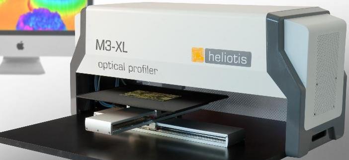
heliProfilerTM M3 / M3-XL - Efficient 3D Measurements
Progress in science and technology is often triggered by advanced measurement techniques. While there is always the possibility of guessing it right, detailed observation and in-depth analysis are indispensable for systematic and productive work. The new M3 Optical Profiler from Heliotis brings superior 3D-metrology to the professional in engineering and science. It has been designed for the most demanding applications in micromechanics, electronics, life sciences and forensics.
Heliotis’ proprietary smart-pixel CMOS-sensor and its “parallel Optical Coherence Tomography” give the M3 an edge in terms of measurement speed and precision on almost any surfaces. The instrument has been engineered for productivity and reliability. It is manufactured in Switzerland for long lasting reliability.
Specifications for M3-XL Optical Profiler
Measuring module
3D-Sensor | Proprietary smart pixel sensor heliSenseTM S3with in-pixel signal processing of up to 1 million 2D-slices per second |
| 2D-Camera | Live-view supports navigation on sample |
| Light source | Standard: Superluminescent Light Emitting Diode (λcenter= 800 nm, Δλ = 40 nm, Poptical = 8 mW) |
| Field of View | 0.6 x 0.6 mm (standard configuration) |
| NA | 0.4 (standard configuration) |
| Working distance | 2.8 mm (standard configuration) |
| Vertical resolution | 1 μm (standard configuration, 20 nm optional) |
| Lateral resolution | 2 μm (standard configuration) |
Scan modules
Z-axis | 20 mm vertical scan range 100 nm resolution Up to 50 mm per second |
| XY-table | 300 x 400 mm positioning range 1 μm resolution (100 nm optional) Up to 100 mm per second |
Software
Graphical User Interface | Configuration and control of the system Navigation via 2D-live-view Graphical representation of 3D-topography and profiles Data processing and analysis Data management and storage Automation of measurement tasks (recipes) |
| Application Programming Interface | C++, Python and LabView 8.x (scanner control, 3D-camera configuration and readout, 2D-camera configuration and readout, data processing algorithms |
Applications
Providing fast and robust 3D-metrological data, Heliotis' unique technology is capable of bringing innovations to many different fields - limited only by your imagination.
To explore what our technology can do for you, please send us a short description of your measurement task. We will gladly perform test measurements of your samples free of charge.
Electronics, Technical Surfaces
CSPs and micro-BGAs continue to increase the packaging density of PCBs, but the ever shrinking pad sizes make it harder to ensure the reliability of the solder joints. Advanced 3D-profiling provides reliable data on solder height and solder volume to fine-tune the screen printer configuration, monitor process statistics for SPC and increase First Pass Yield. Likewise, the requirement on technical surfaces typically increases with miniaturization as surfaces roughness become more significant and tolerances smaller. True 3D-inspection yields unambiguous quality data and can provide feedback to the manufacturing process. |
Micro-mechanics, Micro-optics
Miniaturization allows for innovative products with superior performance at reduced costs. Devices such as MEMS and micro-optics make use of production techniques originally developed for integrated circuits. With dimensions down to the micro-meter range, conventional inspection systems are no longer appropriate - especially where three dimensional accuracy needs to be verified. The M3 helps the developer to quickly gain an in-depth understanding of the true 3D shapes produced by a set of process parameters. The M3 takes 3D profiles of almost any material (reflective and diffusive). For inspection no preparation of the devices is necessary. |
Life Science
The M3 delivers quantitative topological and tomographic data of biological samples in high resolution. Its non-invasive and non-contact measurement principle p-OCT works with non-ionizing visible or near infrared light. In contrast to scanning electron microscopes, the samples do not need to be coated or evacuated. Thus, the M3 allows for rapid characterization of biological samples and even delivers quantitative 3D data. |
Forensics & Security Solutions
Fnology is used for comparing cartridge cases from crime scenes, demonstrating superior performance over legacy 2D systems. Furthermore, the detailed 3D-metrology is instrumental in detecting counterfeits and forgery. There are numerous possibilities for innovative security products based on micro 3D-features. The M3 is the perfect tool for creating it. |
產(chǎn)品咨詢(xún)
請(qǐng)?zhí)顚?xiě)您的姓名:*
請(qǐng)?zhí)顚?xiě)您的電話(huà):*
請(qǐng)?zhí)顚?xiě)您的郵箱:*
請(qǐng)?zhí)顚?xiě)您的單位/公司名稱(chēng):*
請(qǐng)?zhí)岢瞿膯?wèn)題:*
您需要的服務(wù):
中國(guó)粉體網(wǎng)保護(hù)您的隱私權(quán):請(qǐng)參閱 我們的保密政策 來(lái)了解您數(shù)據(jù)的處理以及您這方面享有的權(quán)利。 您繼續(xù)訪(fǎng)問(wèn)我們的網(wǎng)站,表明您接受 我們的使用條款
自動(dòng)型
TOF-4R05
BA-100 M


